搜索附件  
头雁微网 附件中心 技术应用 情报信息 Wiley.Advanced.FPGA.Design.Jun.2007: Wiley.Advanced.FPGA.Design.Jun.2007.part1.rar
板块导航
附件中心&附件聚合2.0
For Discuz! X3.5 © hgcad.com

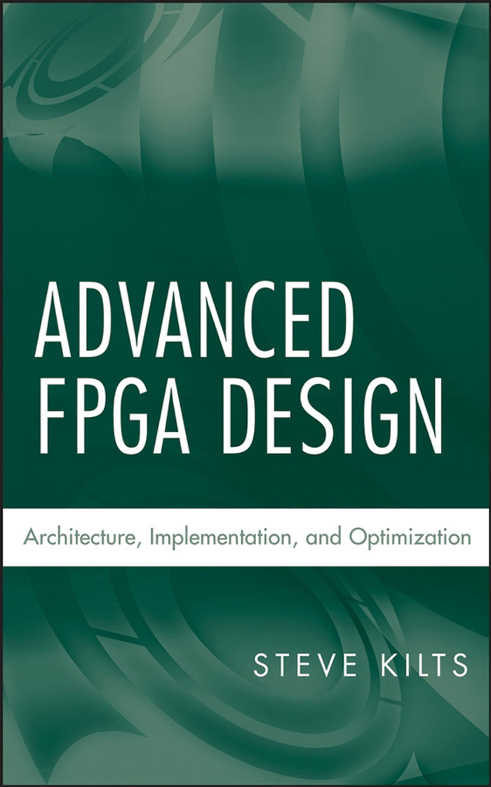
Wiley.Advanced.FPGA.Design.Jun.2007: Wiley.Advanced.FPGA.Design.Jun.2007.part1.rar


Wiley.Advanced.FPGA.Design.Jun.2007:
Copyright # 2007 by John Wiley & Sons, Inc. All rights reserved.
Published by John Wiley & Sons, Inc., Hoboken, New Jersey.
Published simultaneously in Canada.
No part of this publication may be reproduced, stored in a retrieval system, or transmitted in any
form or by any means, electronic, mechanical, photocopying, recording, scanning, or otherwise,
except as permitted under Section 107 or 108 of the 1976 United States Copyright Act, without
either the prior written permission of the Publisher, or authorization through payment of the
appropriate per-copy fee to the Copyright Clearance Center, Inc., 222 Rosewood Drive, Danvers,
MA 01923, 978-750-8400, fax 978-646-8600, or on the web at www.copyright.com.
Requests to the Publisher for permission should be addressed to the Permissions Department,
John Wiley & Sons, Inc., 111 River Street, Hoboken, NJ 07030, (201) 748-6011,
fax (201) 748-6008.
Limit of Liability/Disclaimer of Warranty: While the publisher and author have used their best
efforts in preparing this book, they make no representations or warranties with respect to
the accuracy or completeness of the contents of this book and specifically disclaim any implied
warranties of merchantability or fitness for a particular purpose. No warranty may be created
or extended by sales representatives or written sales materials. The advice and strategies contained
herein may not be suitable for your situation. You should consult with a professional where
appropriate. Neither the publisher nor author shall be liable for any loss of profit or any
other commercial damages, including but not limited to special, incidental, consequential,
or other damages.
For general information on our other products and services please contact our Customer Care
Department within the U.S. at 877-762-2974, outside the U.S. at 317-572-3993 or
fax 317-572-4002.
Wiley also publishes its books in a variety of electronic formats. Some content that appears in print,
however, may not be available in electronic format.
Library of Congress Cataloging-in-Publication Data
Kilts, Steve, 1978-
Advanced FPGA design: Architecture, Implementation, and Optimization/
by Steve Kilts.
p. cm.
Includes index.
ISBN 978-0-470-05437-6 (cloth)
1. Field programmable gate arrays- -Design and construction.
I. Title.
TK7895.G36K55 2007
621.3905- -dc22
2006033573
Printed in the United States of America
Contents
Preface xiii
Acknowledgments xv
1. Architecting Speed 1
1.1 High Throughput 2
1.2 Low Latency 4
1.3 Timing 6
1.3.1 Add Register Layers 6
1.3.2 Parallel Structures 8
1.3.3 Flatten Logic Structures 10
1.3.4 Register Balancing 12
1.3.5 Reorder Paths 14
1.4 Summary of Key Points 16
2. Architecting Area 17
2.1 Rolling Up the Pipeline 18
2.2 Control-Based Logic Reuse 20
2.3 Resource Sharing 23
2.4 Impact of Reset on Area 25
2.4.1 Resources Without Reset 25
2.4.2 Resources Without Set 26
2.4.3 Resources Without Asynchronous Reset 27
2.4.4 Resetting RAM 29
2.4.5 Utilizing Set/Reset Flip-Flop Pins 31
2.5 Summary of Key Points 34
3. Architecting Power 37
3.1 Clock Control 38
3.1.1 Clock Skew 39
3.1.2 Managing Skew 40
vii
3.2 Input Control 42
3.3 Reducing the Voltage Supply 44
3.4 Dual-Edge Triggered Flip-Flops 44
3.5 Modifying Terminations 45
3.6 Summary of Key Points 46
4. Example Design: The Advanced Encryption Standard 47
4.1 AES Architectures 47
4.1.1 One Stage for Sub-bytes 51
4.1.2 Zero Stages for Shift Rows 51
4.1.3 Two Pipeline Stages for Mix-Column 52
4.1.4 One Stage for Add Round Key 52
4.1.5 Compact Architecture 53
4.1.6 Partially Pipelined Architecture 57
4.1.7 Fully Pipelined Architecture 60
4.2 Performance Versus Area 66
4.3 Other Optimizations 67
5. High-Level Design 69
5.1 Abstract Design Techniques 69
5.2 Graphical State Machines 70
5.3 DSP Design 75
5.4 Software/Hardware Codesign 80
5.5 Summary of Key Points 81
6. Clock Domains 83
6.1 Crossing Clock Domains 84
6.1.1 Metastability 86
6.1.2 Solution 1: Phase Control 88
6.1.3 Solution 2: Double Flopping 89
6.1.4 Solution 3: FIFO Structure 92
6.1.5 Partitioning Synchronizer Blocks 97
6.2 Gated Clocks in ASIC Prototypes 97
6.2.1 Clocks Module 98
6.2.2 Gating Removal 99
6.3 Summary of Key Points 100
7. Example Design: I2S Versus SPDIF 101
7.1 I2S 101
7.1.1 Protocol 102
7.1.2 Hardware Architecture 102
viii Contents
7.1.3 Analysis 105
7.2 SPDIF 107
7.2.1 Protocol 107
7.2.2 Hardware Architecture 108
7.2.3 Analysis 114
8. Implementing Math Functions 117
8.1 Hardware Division 117
8.1.1 Multiply and Shift 118
8.1.2 Iterative Division 119
8.1.3 The Goldschmidt Method 120
8.2 Taylor and Maclaurin Series Expansion 122
8.3 The CORDIC Algorithm 124
8.4 Summary of Key Points 126
9. Example Design: Floating-Point Unit 127
9.1 Floating-Point Formats 127
9.2 Pipelined Architecture 128
9.2.1 Verilog Implementation 131
9.2.2 Resources and Performance 137
10. Reset Circuits 139
10.1 Asynchronous Versus Synchronous 140
10.1.1 Problems with Fully Asynchronous Resets 140
10.1.2 Fully Synchronized Resets 142
10.1.3 Asynchronous Assertion, Synchronous Deassertion 144
10.2 Mixing Reset Types 145
10.2.1 Nonresetable Flip-Flops 145
10.2.2 Internally Generated Resets 146
10.3 Multiple Clock Domains 148
10.4 Summary of Key Points 149
11. Advanced Simulation 151
11.1 Testbench Architecture 152
11.1.1 Testbench Components 152
11.1.2 Testbench Flow 153
11.1.2.1 Main Thread 153
11.1.2.2 Clocks and Resets 154
11.1.2.3 Test Cases 155
Contents ix
11.2 System Stimulus 157
11.2.1 MATLAB 157
11.2.2 Bus-Functional Models 158
11.3 Code Coverage 159
11.4 Gate-Level Simulations 159
11.5 Toggle Coverage 162
11.6 Run-Time Traps 165
11.6.1 Timescale 165
11.6.2 Glitch Rejection 165
11.6.3 Combinatorial Delay Modeling 166
11.7 Summary of Key Points 169
12. Coding for Synthesis 171
12.1 Decision Trees 172
12.1.1 Priority Versus Parallel 172
12.1.2 Full Conditions 176
12.1.3 Multiple Control Branches 179
12.2 Traps 180
12.2.1 Blocking Versus Nonblocking 180
12.2.2 For-Loops 183
12.2.3 Combinatorial Loops 185
12.2.4 Inferred Latches 187
12.3 Design Organization 188
12.3.1 Partitioning 188
12.3.1.1 Data Path Versus Control 188
12.3.1.2 Clock and Reset Structures 189
12.3.1.3 Multiple Instantiations 190
12.3.2 Parameterization 191
12.3.2.1 Definitions 191
12.3.2.2 Parameters 192
12.3.2.3 Parameters in Verilog-2001 194
12.4 Summary of Key Points 195
13. Example Design: The Secure Hash Algorithm 197
13.1 SHA-1 Architecture 197
13.2 Implementation Results 204
14. Synthesis Optimization 205
14.1 Speed Versus Area 206
14.2 Resource Sharing 208
x Contents
14.3 Pipelining, Retiming, and Register Balancing 211
14.3.1 The Effect of Reset on Register Balancing 213
14.3.2 Resynchronization Registers 215
14.4 FSM Compilation 216
14.4.1 Removal of Unreachable States 219
14.5 Black Boxes 220
14.6 Physical Synthesis 223
14.6.1 Forward Annotation Versus Back-Annotation 224
14.6.2 Graph-Based Physical Synthesis 225
14.7 Summary of Key Points 226
15. Floorplanning 229
15.1 Design Partitioning 229
15.2 Critical-Path Floorplanning 232
15.3 Floorplanning Dangers 233
15.4 Optimal Floorplanning 234
15.4.1 Data Path 234
15.4.2 High Fan-Out 234
15.4.3 Device Structure 235
15.4.4 Reusability 238
15.5 Reducing Power Dissipation 238
15.6 Summary of Key Points 240
16. Place and Route Optimization 241
16.1 Optimal Constraints 241
16.2 Relationship between Placement
and Routing 244
16.3 Logic Replication 246
16.4 Optimization across Hierarchy 247
16.5 I/O Registers 248
16.6 Pack Factor 250
16.7 Mapping Logic into RAM 251
16.8 Register Ordering 251
16.9 Placement Seed 252
16.10 Guided Place and Route 254
16.11 Summary of Key Points 254
17. Example Design: Microprocessor 257
17.1 SRC Architecture 257
17.2 Synthesis Optimizations 259
17.2.1 Speed Versus Area 260
Contents xi
17.2.2 Pipelining 261
17.2.3 Physical Synthesis 262
17.3 Floorplan Optimizations 262
17.3.1 Partitioned Floorplan 263
17.3.2 Critical-Path Floorplan: Abstraction 1 264
17.3.3 Critical-Path Floorplan: Abstraction 2 265
18. Static Timing Analysis 269
18.1 Standard Analysis 269
18.2 Latches 273
18.3 Asynchronous Circuits 276
18.3.1 Combinatorial Feedback 277
18.4 Summary of Key Points 278
19. PCB Issues 279
19.1 Power Supply 279
19.1.1 Supply Requirements 279
19.1.2 Regulation 283
19.2 Decoupling Capacitors 283
19.2.1 Concept 283
19.2.2 Calculating Values 285
19.2.3 Capacitor Placement 286
19.3 Summary of Key Points 288
Appendix A 289
Appendix B 303
Bibliography 319
Index 321
:11bb
:11bb
不错的资料,感谢楼主!!!:cacakiki13de
:11bb :11bb :11bb :11bb :11bb
:27bb 很好的资料,值得学习下!
:30bb :11bb :27bb :29bb :23de
很好的资料,非常感谢楼主的共享!!!
很好的资料,非常感谢楼主的共享!!!
:11bb :11bb :11bb :11bb :11bb :11bb :11bb
不错的
不错的资料,感谢楼主!!!:30bb
:30bb :30bb :30bb :30bb :30bb :30bb :30bb
good,very good,thanks
感谢非常,非常感谢~~~~~~~~~~~~~!!!!!!!!!!!!
很好的资料,非常感谢楼主的共享!!!
真是好资料,搂主一定是这方面专家,学习
真的是很好的资料,感谢楼主的共享!!!
真的是很好的资料,感谢楼主的共享!!!
可惜下载未必能去看
这是伤心啊
不错的资料:31bb
呵呵~~谢谢楼主~~~
多谢楼主分享{:7_1235:}
thanks!!!!!!!!!!!!!!
不错不错,谢谢楼主分享
客服中心 搜索
关于我们
关于我们
关注我们
联系我们
帮助中心
资讯中心
企业生态
社区论坛
服务支持
资源下载
售后服务
推广服务
关注我们
官方微博
官方空间
官方微信
返回顶部